垂直氮化镓(vGaN)
先锋技术,引领变革
AI和电气化应用的性能飞跃

AI和电气化的突破性技术
安森美的垂直氮化镓(vGaN)技术是一项突破性的功率半导体技术,带来创纪录的效率、功率密度和耐用性,满足AI和电气化时代的应用需求。
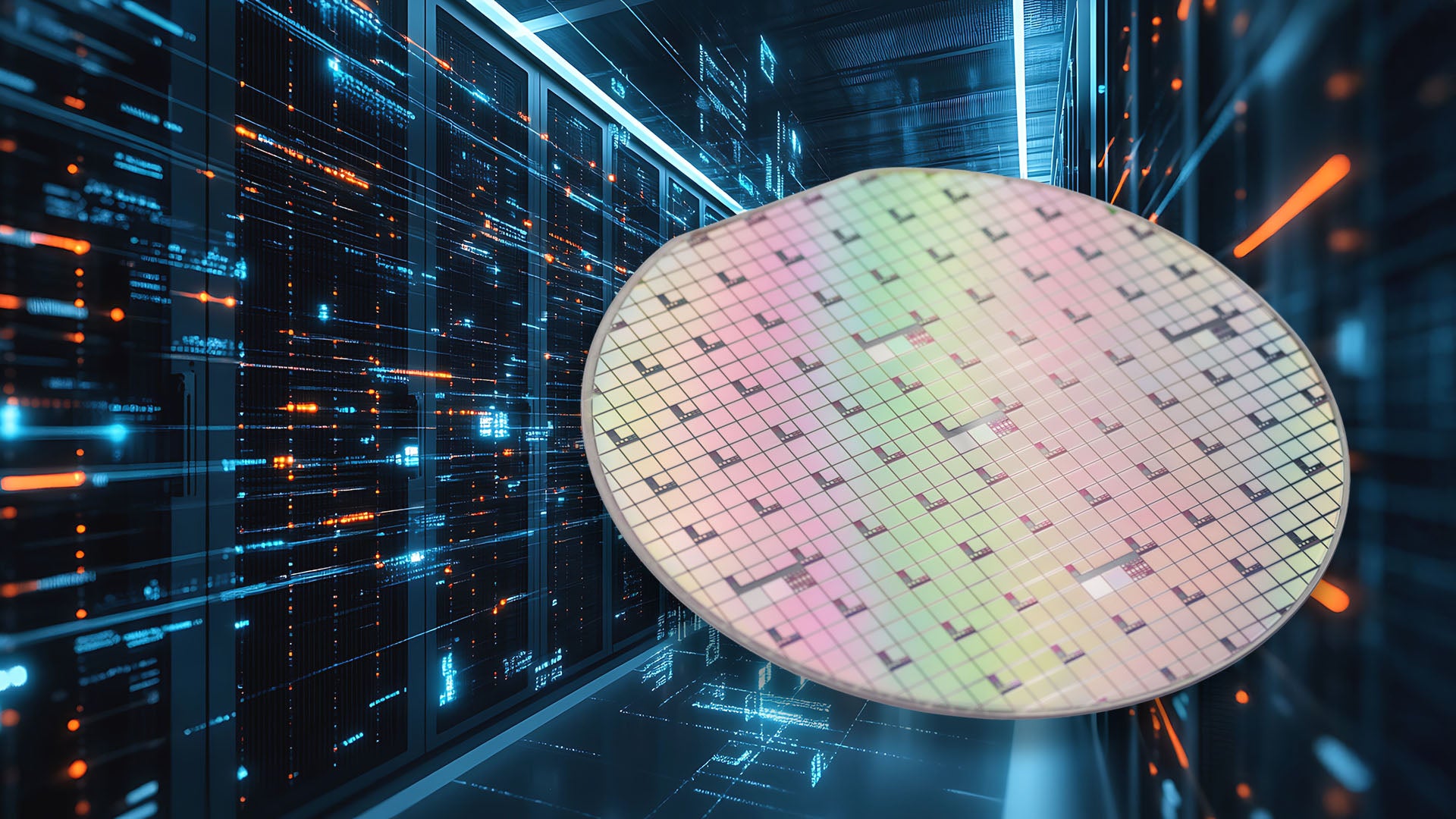
这一技术由安森美位于纽约州锡拉丘兹的工厂研发和制造。新一代“GaN-on-GaN”功率半导体能够使电流垂直流经芯片而非沿表面横向流动,从而在更小尺寸的双面散热封装中实现优秀的性能表现。
精选资源
探索我们为您精选的垂直氮化镓资源,让您的设计之路更加智能、快捷,信心倍增。
安森美垂直氮化镓视频介绍
功率密度是最新的制胜之道。垂直氮化镓技术,安森美专有工艺,带来更高电压、更快开关、和创纪录的高效率,适用于AI数据中心、电动汽车和可再生能源系统。
安森美vGaN特性
更高功率密度
可达1200V及以上
更高能效
更低的能量损耗和发热量,效率提升50%以上
更紧凑的系统
终端系统占位更少、重量更轻
一流的生产制造工艺
纽约州锡拉丘兹工厂占地66,000平方英尺,掌握专有技术工艺,在氮化镓衬底上直接生成氮化镓层
创新封装技术
双面散热封装
引领未来
vGaN技术支持的开关频率远高于传统方案
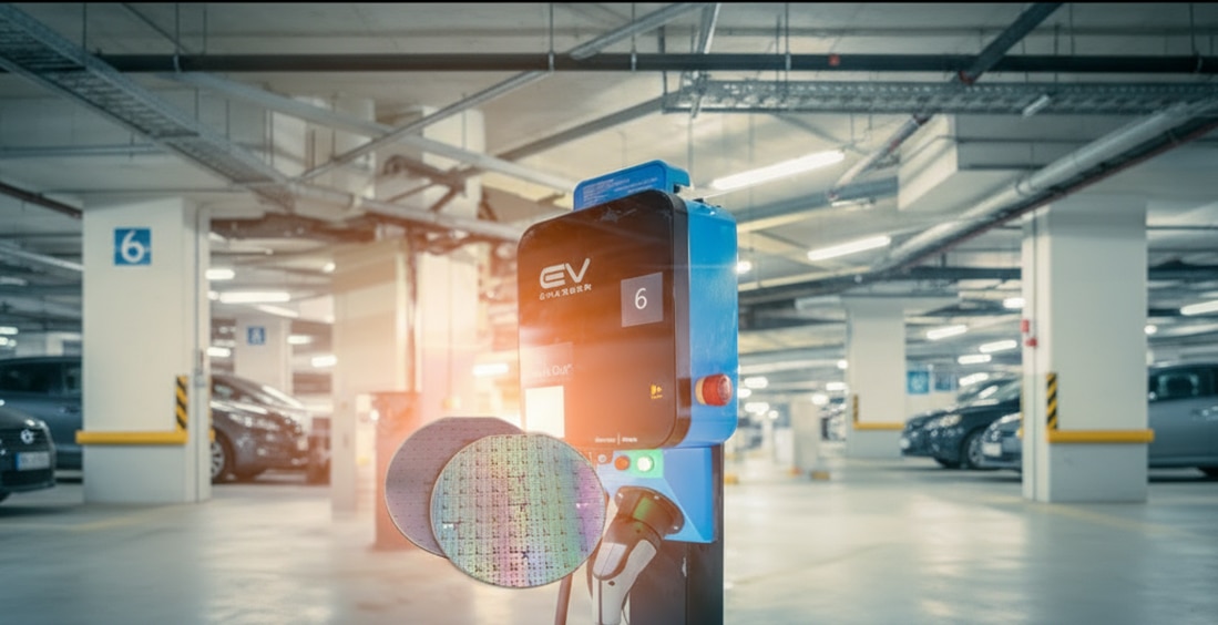
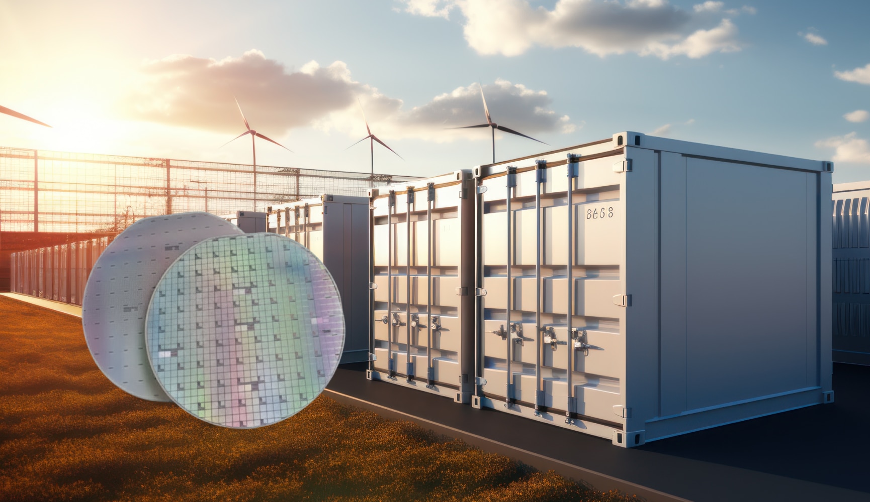
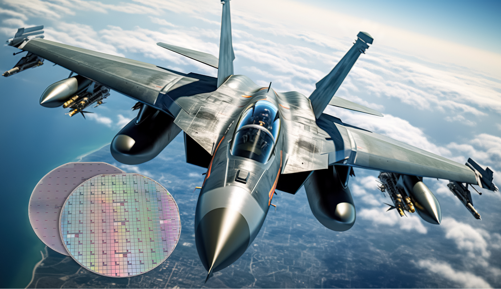
关键技术应用

精选文章
浏览我们的新闻公告和博客文章,为您的下一次设计注入灵感。
October 30, 2025
安森美发布垂直氮化镓(GaN)半导体:为人工智能(AI)与电气化领域带来突破性技术
October 30, 2025
安森美垂直氮化镓(vGaN) 技术:综合常见问题解答
支持服务和资讯
如果您对安森美的任一技术感兴趣,欢迎前往我们的问答数据库查阅相关文章。

智能电源
联系我们进一步了解安森美的氮化镓解决方案。

支持
为您提供多种联系方式,让您以最便捷的方式获得支持服务。

资讯
掌握安森美氮化镓相关的最新产品、活动和前沿技术动态。